


What is Gallium Nitride (GAN)
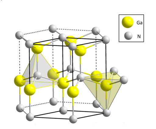
Gallium nitride is a compound composed of gallium (atomic number 31) and nitrogen (atomic number 7).It is a wide-bandgap semiconductor material with a stable hexagonal crystal structure.The forbidden band refers to the energy required for electrons to escape from the nuclear orbit. The forbidden band width of gallium nitride is 3.4eV, which is more than three times that of silicon, so gallium nitride has wide bandgap characteristics (WBG).
GAN material properties
Compared with Si, GAN has the characteristics of large band gap, high breakdown field strength, high electron mobility, and high electron saturation drift velocity.

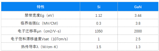
Bandgap width: The bandgap width of a semiconductor is related to the strength of chemical bonds between lattice atoms. Stronger chemical bonds mean that it is more difficult for electrons to jump from one position to the next, so semiconductor materials with larger bandgap widths have lower The intrinsic leakage current and higher operating temperature of
Critical field strength: Stronger chemical bonds lead to a larger band gap, which also leads to a higher critical breakdown electric field when causing avalanche breakdown.
Electron mobility: The breakdown field strength of GaN is 10 times that of Si, and the electron mobility is about 1.5 times that of Si, which can effectively reduce the on-resistance Rdson.In other words, for the same on-resistance Rdson, the GaN chip area is smaller, which is beneficial to reducing the parasitic parameters of the device.
Electron saturation drift speed: The electron saturation drift speed represents the upper limit that the overall electron drift speed can reach as the electric field increases, and has an important impact on the operating frequency of the device. The electron saturation drift speed of GaN is 2.5 times that of Si, which can significantly increase the operating frequency of the device.
Basic structure of GAN transistor
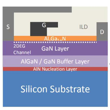
Structurally speaking, GAN devices are mainly lateral structures and are divided from bottom to top into substrate, buffer layer, GaN epitaxy layer and AlGaN barrier layer. A polarization effect occurs at the interface between the AlGaN barrier layer and the GaN epitaxial layer, forming a layer of electrons in GaN, called a two-dimensional electron gas (2DEG). 2DEG, as a natural conductive channel, keeps GaN HEMT normally open and is a depletion mode (D-Mode) device.

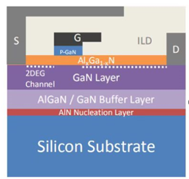
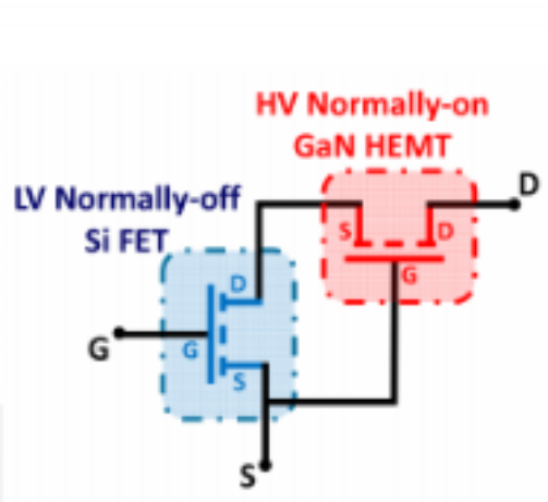
When using D-Mode devices in power electronic converters, it is necessary to add a negative voltage turn-off device between G and S. This will increase the complexity of the drive circuit and also bring about the hidden danger of device shoot-through.To deal with this problem, the industry usually has two solutions. One is to use a cascode structure, and the other is to add P-type gallium nitride to the gate to form an enhancement mode (normally closed) transistor, as shown in the figure below. The cascaded normally-off device is an enhancement-mode SI FET and a depletion-mode GAN connected in series. The gate-level driver is directly connected to the low-voltage MOS instead of the GAN. The current mainstream technology is to use the P-GaN process structure enhancement-mode transistor, with the GaN gate A PGaN layer is placed underneath. PGaN causes the GaN epitaxial layer under the gate to form a depletion region, blocking 2DEG.As the voltage of Vgs gradually increases, the 2DEG under the gate gradually recovers, and the current Ids that the channel can conduct becomes larger.When Ids reaches a specified value, the corresponding Vgs is called the threshold voltage Vth.

GaN transistor electrical characteristics
Differences in material properties and device structures lead to differences in electrical properties between GaN and Si MOSFETs. The following is the comparison data between GAN and SI.

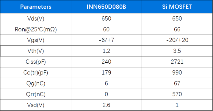
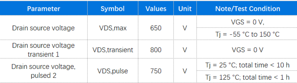
1): Pressure resistance characteristics
Occasional events such as lightning strikes, startup or load switching may cause the device's Vds overvoltage. In actual tests, GaN can withstand higher voltages than SI.

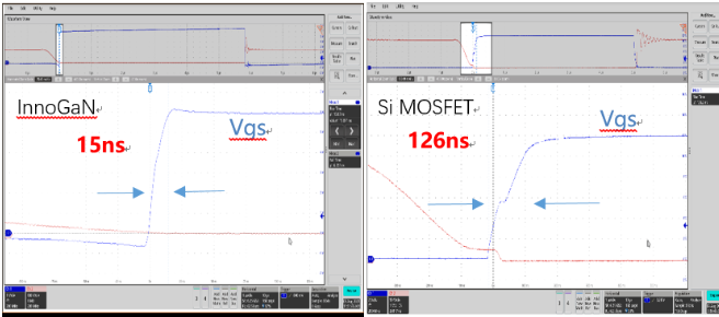
2): Switching speed
The switching speed is mainly affected by Ciss (Ciss=Cgs+Cgd). The larger Ciss is, the slower Vgs changes and the slower the switching speed.Comparing GaN and Si MOSFETs with similar specifications, its Ciss is less than 1/10 of Si MOSFET.Reducing junction capacitance is beneficial to increasing switching speed, reducing losses and enabling high-frequency operation.After testing, GaN's conduction speed is significantly faster, effectively shortening the overlap time of Vds and Id, thereby reducing switching losses.The high-frequency operation of the device can effectively reduce the size of the inductor, transformer and capacitor in the circuit, and significantly increase the power density.

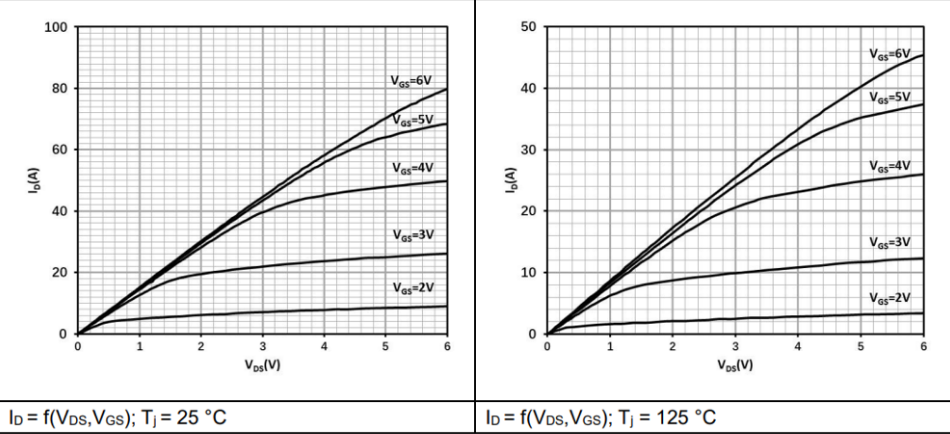
3): Driving characteristics
The drive level of GaN HEMT is different from that of Si MOSFET.The product specification specifies the Vgs level range to ensure that the gate is not damaged.In addition, Vgs determines the degree of device channel opening.It can be seen from the output characteristic curve that the larger the Vgs, the more fully the channel is opened and the stronger the current flow capacity of the device is.

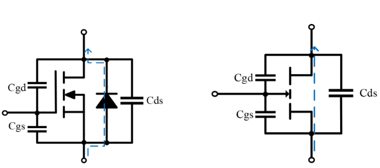
4): Reverse characteristics
Si MOSFET relies on the body diode to achieve reverse conduction.During the process from forward conduction to reverse cut-off of the diode, due to the charge storage effect, a reverse current will flow, which is called the reverse recovery of the diode.This process will bring additional losses and noise, hindering circuit efficiency improvement and EMI design. GaN HEMT does not have a body diode and relies on its own channel to achieve reverse conduction, thus avoiding problems caused by reverse recovery.