





As fast-charging standards continue to advance across smartphones, laptops, industrial electronics, and medical systems, the GaN-powered charger market is experiencing rapid global growth.
Manufacturers are increasingly adopting GaN technology to meet the demand for higher power density, lower energy loss, and more compact designs, particularly when developing high-performance GaN chargers for medical device applications.
This article examines GaN technology from three perspectives — material properties, efficiency mechanisms, and thermal management — to explain why it is becoming a key technology in next-generation charging systems.
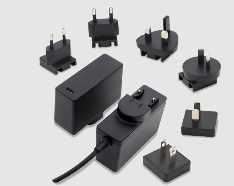
What Does GaN Mean for Chargers?
Silicon semiconductor technology is approaching its physical limitations in high-frequency, high-voltage, and high-power-density applications. Gallium nitride (GaN), as a wide-bandgap semiconductor, provides several important material advantages:
(1) Higher Breakdown Electric Field Strength
The critical electric field strength of GaN is approximately 3 MV/cm, nearly an order of magnitude higher than that of silicon[1]. This enables devices to maintain high voltage ratings while using smaller transistor structures.
(2) Higher Electron Saturation Velocity
Charge carriers can switch significantly faster in GaN devices, enabling much higher switching frequencies than conventional silicon transistors.
(3) Comparable Thermal Conductivity
GaN has a thermal conductivity of approximately 130–253 W/m·K for bulk single-crystal material, compared with silicon’s ~150 W/m·K[2].
The two materials are within the same general range, and GaN’s practical thermal advantage in chargers comes primarily from generating substantially less heat during operation.
(4) Higher Temperature Tolerance
GaN devices can tolerate significantly higher junction temperatures than silicon devices, often exceeding 200°C under controlled operating conditions[3].
These material characteristics directly translate into real-world advantages for chargers: higher efficiency, lower thermal losses, and more compact product designs.
Why Are GaN Chargers Better?
Traditional silicon-based chargers typically achieve energy conversion efficiencies around 85–88%, while high-quality GaN chargers can exceed 90%, with some advanced designs approaching 95% peak efficiency under optimized conditions[4].
This improvement is primarily driven by GaN’s ability to reduce two major forms of power loss:
1. Faster Switching Speed
The transition between the “on” and “off” states of a transistor is a primary source of energy loss in power conversion systems. Silicon transistors generally switch within tens of nanoseconds, while GaN devices can operate in the low single-digit nanosecond range.
This significantly reduces switching losses and improves overall charger efficiency.
2. Lower On-Resistance (RDS(on))
GaN devices can achieve significantly lower on-resistance (RDS(on)) than comparable silicon devices, reducing conduction losses and improving power conversion efficiency.
Lower resistance also means less energy is dissipated as heat during operation, which is one reason GaN chargers often exhibit lower surface temperatures than conventional chargers.
3. Elimination of Reverse Recovery Losses
Traditional silicon MOSFETs contain intrinsic body diodes that generate reverse recovery losses during switching dead time. GaN transistors do not rely on a conventional body diode structure, allowing current to flow with near-zero reverse recovery losses.
This eliminates one of the major efficiency limitations found in silicon-based charger designs.
4. Support for High-Frequency Operation
Unlike traditional silicon solutions that are limited to kHz-level switching, GaN semiconductors excel in high-frequency environments, effectively reaching MHz ranges to optimize power conversion.
Higher switching frequency enables:
- Smaller transformers and passive components
- Reduced magnetic component size
- Faster transient response
- Increased overall power density
This is a major reason why modern GaN chargers can deliver high wattage output while remaining compact and lightweight.
Are GaN Chargers Safe?
Another common question among consumers is: Are GaN chargers safe?
When properly designed and certified, GaN chargers are considered highly safe and reliable. In many cases, GaN chargers can actually improve safety performance because they generate less excess heat than conventional silicon chargers.
However, charger safety depends not only on the semiconductor material itself, but also on circuit protection design, thermal management architecture, component quality, isolation design, compliance testing, and certifications.
High-quality GaN chargers typically incorporate multiple protection mechanisms, including OVP, OCP, OTP, and SCP.
For industrial and medical-related applications, additional safety standards and long-term reliability validation are especially important.
GaN Chargers from UE Electronic
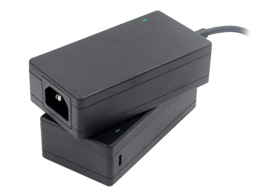
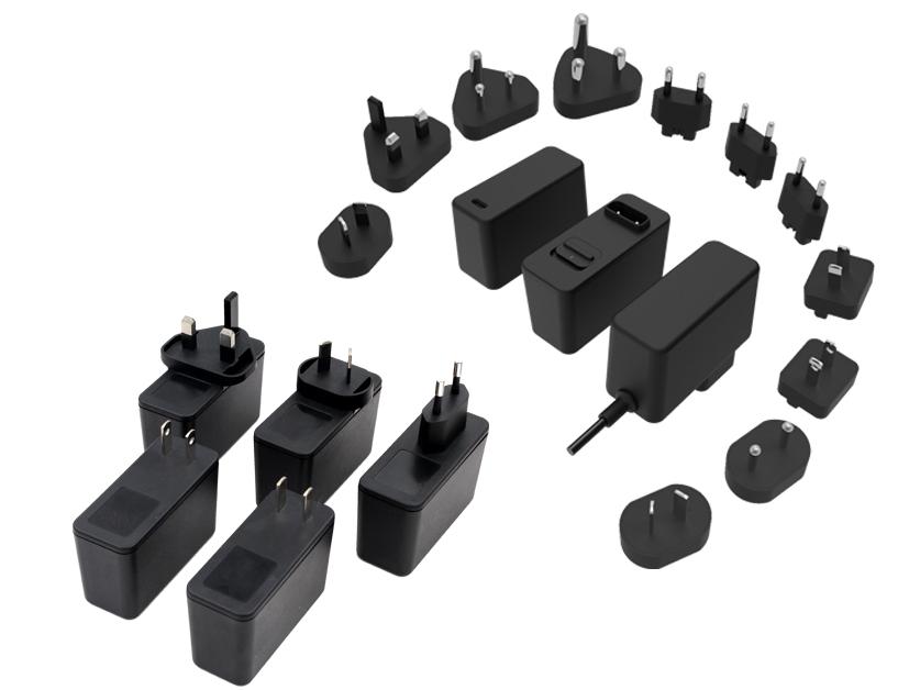
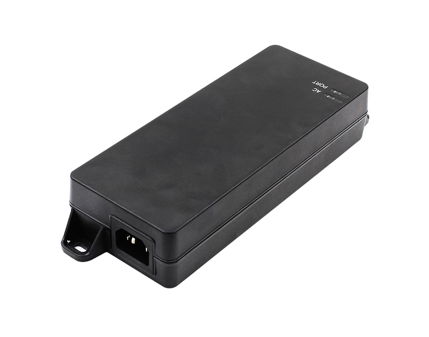
For equipment manufacturers and system integrators seeking high-efficiency, compact GaN power solutions, our UES100B/UES100C-SPCZ offers an optimized balance of efficiency, compactness, and medical-grade safety.
It supports mainstream fast charging protocols, including USB PD3.1 & PD3.0, QC4.0+/3.0/2.0, and is capable of fast charging a wide range of devices, such as laptops, tablets, smartphones, 5G CPE, and portable medical equipment:
(1) Medical-Grade Safety Isolation
Features 2 MOPP isolation protection with extremely low leakage current, which fulfills the strict requirements for GaN chargers for medical device scenarios involving human contact.
(2) Broad Global Safety Certifications
It complies with major international medical and IT safety standards, including UL (ANSI/AAMI ES60601-1), TÜV SUD/Mark (EN60601-1), CB (IEC60601-1), and CE (EN62368-1). This ensures compliance with both medical and information technology equipment safety requirements.
(3) High Power Density and Lower Power Consumption
It achieves a balance of 100W of high-power output (20V/5A) and compact dimensions (109.5 × 56.5 × 32.0 mm).
Standby power consumption is ≤0.15W, outperforming the EU ErP Lot 6 standard (typically <0.3W) and helping reduce unnecessary energy consumption.
(5) Harsh Environment Adaptability
The adapter supports altitudes up to 5000 meters; therefore, it is suitable for plateaus and other high-altitude environments.
(6) Extended Operational Lifespan
Mean Time Between Failures (MTBF) is up to 100,000 hours at 25°C, reflecting the long-term reliability requirements expected in industrial and medical-grade applications.
Conclusion
Compared with conventional silicon-based chargers, GaN solutions offer clear advantages in switching efficiency, thermal management, compactness, and long-term reliability.
For industrial, consumer, and medical applications requiring stable high-performance charging, UE Electronic is your reliable partner, delivering efficient and future-ready power adapter solutions.
References
[1] Newark. “Wide Bandgap Semiconductor: The Future of SiC and GaN Technology.” Accessed 30 October 2026. https://www.newark.com/technical-resources/articles/wide-bandgap-semiconductor-the-future-of-sic-and-gan-technology
[2] PatSnap Eureka. “Thermal Conductivity Showdown: SiC vs GaN vs Silicon.” Accessed 30 October 2026. https://eureka.patsnap.com/article/thermal-conductivity-showdown-sic-vs-gan-vs-silicon
[3] Microchip USA. “GaN and SiC: The Power Electronics Revolution Leaving Silicon Behind.” Accessed 30 October 2026. https://www.microchipusa.com/industry-news/gan-and-sic-the-power-electronics-revolution-leaving-silicon-behind
[4] Anker. “High-Efficiency 45W USB-C Charger.” Accessed 30 October 2026. https://www.anker.com/blogs/chargers/high-efficiency-45w-usb-c-charger