





Lightning strikes are a natural phenomenon. When lightning strikes the ground or an obstacle, an instantaneous surge voltage will enter the power supply through the transmission system (such as power lines/antennas/networks). This abnormal energy can easily cause internal damage to the product. The component is damaged. In addition, in real life, similar instantaneous voltage surges may occur when switching power switches and plugging and unplugging plugs.
In order to effectively verify the product's tolerance to lightning strike protection, IEC has set lightning strike test specifications (IEC-61000-4-5) for different products. Table XNUMX shows the specifications for different products.

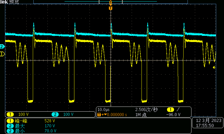
In order to simulate the lightning waveform and energy, the test methods are mainly divided into the following two types: open circuit voltage (refer to Figure 2), and short circuit current (short circuit current; refer to Figure 3)
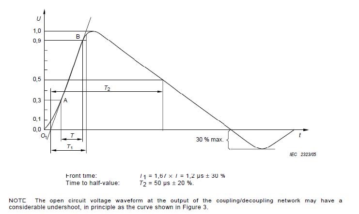
Figure 2 Lightning test method 1: open circuit voltage

Figure 3 Lightning strike test method 2: short circuit current
The lightning strike test items mainly conduct different combination tests on the power supply live wire (L), ground wire (N), and safety ground (E).
There are four main test items (L→E, N→E, L&N→E, L→N), which are divided into two categories based on general design considerations: common mode (Common Mode) and differential mode (Differential mode).
A. L→E, N→E, L&N→E tests belong to Common Mode (Common Mode)
B. L→N test belongs to Differential mode (Differential mode)
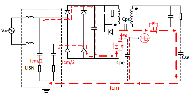
The following is the path of common mode and differential mode during lightning strike testing, as shown in Figure 4.

Figure 4 Common mode and differential mode lightning strike test path diagram
Common mode lightning strike countermeasures:
Common mode lightning energy discharge path, (refer to the green line in Figure 4), first consider the paths across the primary and secondary that may cause lightning flashover or component damage due to insufficient safety distance? (Transformer/Optocoupler/Y -Cap) The selection and design reference for these three components are as follows:
1. Transformer: Because the transformer spans the primary and secondary components, there are different safety distance requirements according to the working voltage. Generally, Class B is used. The component itself needs to pass Hi-POT 3000Vac for the primary and secondary components. Special attention must be paid to the foot distance and Whether the distance between the cores and the number of tapes on each layer of the winding meet the insulation strength.
2. Optocoupler: The distance of the component itself must meet the requirements of safety regulations. There should be no trace under the component during layout to avoid the problem of insufficient distance.
3.Y-Cap: Its own characteristics are high-frequency and low-impedance components. When common-mode lightning strikes are tested, the energy will quickly pass through the path placed by Y-Cap, so the layout of semiconductor components (PWM IC, TL431, OP …) GND trace should avoid the Y Cap lightning energy discharge path to avoid damage to components
Differential mode lightning strike countermeasures:
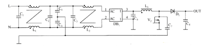
The path through which lightning strike energy flows is mainly in the L and N loops in front of the bridge rectifier. The main countermeasures are as follows: Varistor (MOV) or Spark Gap (lightning strike tube) and other components absorb and inhibit the energy from flowing into the power supply.
1. Thermistor (NTC): Connected in series to the path of L or N, it will increase the impedance value of the loop, thereby reducing the current energy entering the power supply.
2.MOV (Metal Oxide Varistor): Metal oxide or surge absorber, usually connected in parallel to L and N. The component itself is a high-impedance component. Under normal circumstances, there will be no loss, only a slight loss. Leakage current, when the instantaneous high potential of lightning strikes enters the power input terminal and exceeds the collapse voltage of the MOV, an action is taken to suppress the voltage, allowing the instantaneous rising current to flow through the MOV itself for energy absorption, reducing the energy of the lightning strike entering the power supply itself.
3.Spark Gap or Gas Discharge Tube: Used in parallel to both ends of the same primary side of the common mode inductor, the action protection principle for lightning strikes will be triggered when the instantaneous high potential exceeds its rated voltage at both ends of the common mode inductor. Inert gas, at this time, Spark Gap will generate arc discharge, suppressing the energy of the surge and preventing a large amount of energy from entering the power supply.
4. Plan a zigzag copper foil pattern on the layout, with the distance between the two ends about 1mm. When the voltage difference between the two ends of the common mode inductor is too large, tip discharge will occur and the energy will be discharged.
In addition to the above-mentioned design considerations, how to achieve protection against electric shock in Layout is also an important part:
1. Ground wire processing, as shown in Figure XNUMX
A. For the primary side part, the layout sequence of Ground is: Ground of large capacitor → Current sensor → Y-Cap → Primary side transformer auxiliary winding Vcc Ground of capacitor → Ground of PWM IC peripheral components → Ground of PWM IC.
B. Secondary side part: The ground of TL431 is connected to the ground of the second-stage output capacitor.
C. The output pin of the secondary side Y-cap is connected to the ground of the secondary side transformer.

Figure 5 How to handle the ground wire
2. The processing of the high-voltage part of the positive end is shown in Figure XNUMX.
A. The distance between the two lines L and N is more than 2.5mm and the distance from E is more than 4mm.
B. The safe distance between high-voltage copper foil and low-voltage copper foil is more than 1.5mm.
C. The distance between the primary and secondary sides is more than 6mm.