





In recent years, with the continuous improvement of international energy efficiency standards, conventional Schottky diode rectifiers cannot meet the energy efficiency requirements of low-voltage and high-current output specifications (US DoE Level VI, EU CoC V5 Tier 2); even if ultra-low Vf Schottky rectification is used, For special diode rectification, some also need to add heat sinks, which will lead to large PCB space, low power density, low efficiency, high case temperature, and poor user experience.Using synchronous rectification MOS, under the same output current, the loss is very small, which greatly improves the conversion efficiency of the entire machine.
There are many working modes of switching power supply (CCM, DCM, QR, BURST), and the synchronous rectification control IC is a passive receiving synchronization method, so it is difficult to avoid faults under any load and full voltage input conditions. The following are some common problems and improvement measures
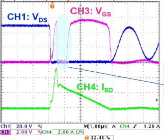
1: The MOS tube is turned on or off in advance
cause:
1) The SR IC_gate driver output is disturbed and turns on in advance.
2) If the internal slope detection circuit of the SR IC is disturbed, it will be turned on in advance or on the first Ring.
3) After the SR IC_gate is turned on, it is interfered by the primary leakage inductance and the DS capacitance oscillation of the MOS and mistakenly triggers the shutdown of the MOS.

Make an impact:
1) The gate of SR MOS is turned off in advance, which will lead to long conduction time of the diode in the body, low efficiency, and high temperature of synchronous MOS.
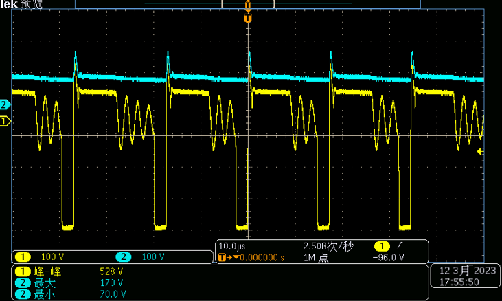
2) Looking at the waveform from primary Vds or secondary Vds, there will be small and large waves (for CCM mode).
solutions:
1) Choose a good SR IC brand
2) Improve PCB layout (for SRIC extrapolated MOS)
3) Adjust the primary absorption RCD circuit, such as absorbing a diode in series with a damping resistor
2: Common problems with primary and secondary MOS
cause:
In CCM, when the primary MOS is turned on, the secondary MOS should be turned off promptly and accurately. When the turn-off delay of the secondary MOS is too long, there is a possibility that the primary MOS and secondary MOS are common.
Make an impact:
The secondary side will generate a large reverse current, which will seriously damage the MOS.
solutions:
1) Choose an SR IC with a very short Turn-off Time Delay
2) Choose appropriate SR MOSFET (use smaller Qg)
3) Increase the Q1_Gate drive resistance and slow down its drive speed
4) Design appropriate secondary RC absorption loop parameters
3: The output voltage drops, the ripple is large, and the load capacity drops.
cause:
(针对PSR 架构下的同步整流应用)针对在高压230Vac条件下其工作频率去到80KHz或以上的PSR IC方案(BCM/QR,频率限制在110KHz),当电源系统工作在低压115V (实际从170Vac以下电压都有机会出现输出掉坑问题。同步MOS没打开,体内二极管已经工作,导致输出电压下降(一个PN结压降)。
Make an impact:
Vout输出电压掉坑,不稳定,纹波大,严重情况下会导致输出电压直接掉到4.2-4.5V,输出电流也下降(只能带到满载的1/2 or 2/3)
solutions:
1) Lowering the transformer inductance and lowering the operating frequency below 80KHz will partially improve it, but it cannot completely solve the problem.
2) Using DCM PSR IC, the operating frequency is below 70KHz.
4: After the output short-circuit SCP, the temperature of the SR MOS tube is high and the input instantaneous power increases.
cause:
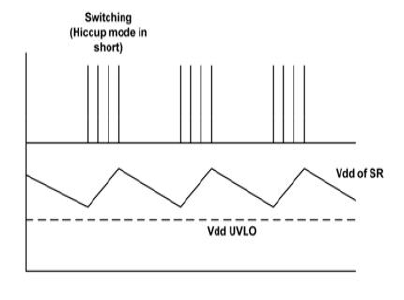
When the output terminal enters short-circuit protection, the primary IC enters HiccupMode. If the VCC power supply is insufficient, the SR MOS enters the UVLO undervoltage protection, and then Isd flows into the diode in the MOS body. At this time, the temperature of the SR MOS rises, and the input instantaneous power increases relatively.

solutions:
- Select a SRIC whose Vo short-circuit protection value is lower than Vdd_UVLO;
- If the SR IC does not have Vo short circuit protection function, you can try to increase the Vcc capacitor capacity.